- 您现在的位置:买卖IC网 > Sheet目录323 > DSP56311EVM (Freescale Semiconductor)KIT EVALUATION FOR DSP56311
ESSI Programming Model
7.5.2 ESSI Control Register B (CRB)
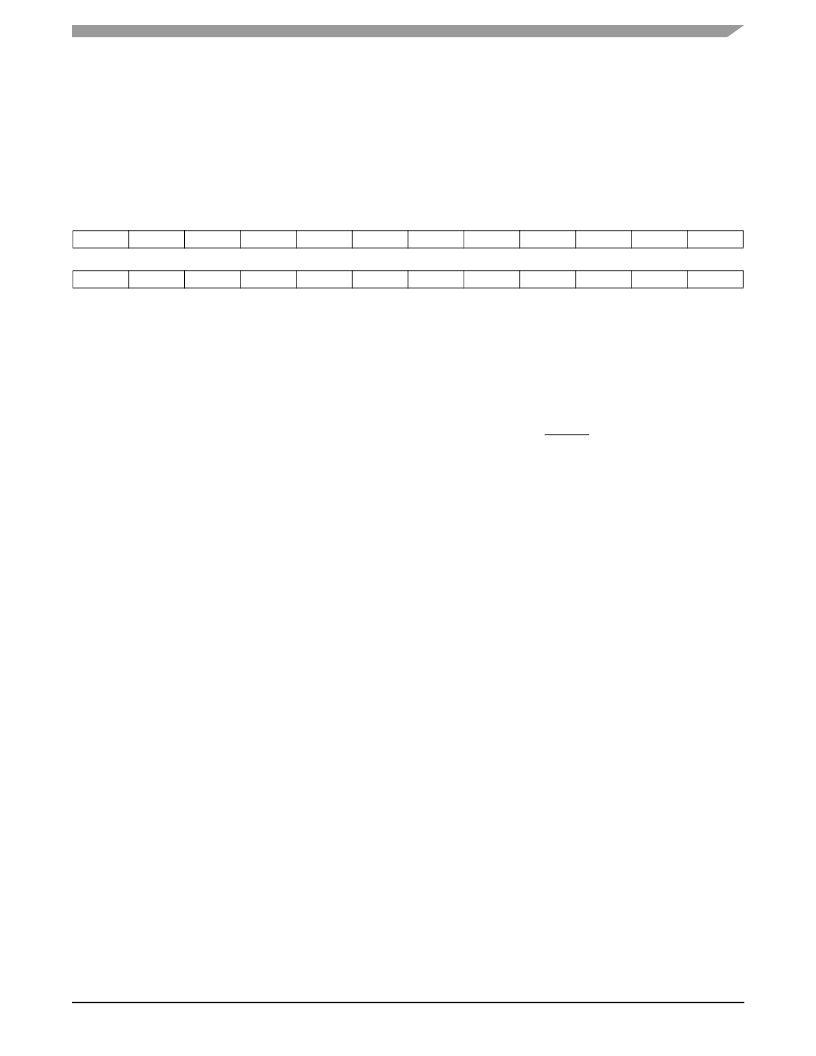
CRB is one of two read/write control registers that direct the operation of the ESSI (see Figure
7-5 ). The CRB bit definitions are presented in Table 7-4 . CRB controls the ESSI multifunction
signals, SC[2–0], which can be used as clock inputs or outputs, frame synchronization signals,
transmit data signals, or serial I/O flag signals.
23
REIE
11
CKP
22
TEIE
10
FSP
21
RLIE
9
FSR
20
TLIE
8
FSL1
19
RIE
7
FSL0
18
TIE
6
SHFD
17
RE
5
SCKD
16
TE0
4
SCD2
15
TE1
3
SCD1
14
TE2
2
SCD0
13
MOD
1
OF1
12
SYN
0
OF0
(ESSI0 X:$FFFFB6, ESSI1 X:$FFFFA6)
Figure 7-5. ESSI Control Register B (CRB)
The CRB contains the serial output flag control bits and the direction control bits for the serial
control signals. Also in the CRB are interrupt enable bits for the receiver and the transmitter. Bit
settings of the CRB determines how many transmitters are enabled: 0, 1, 2, or 3. The CRB
settings also determine the ESSI operating mode. Either a hardware RESET signal or a software
The ESSI has two serial output flag bits, OF1 and OF0. The normal sequence follows for setting
output flags when transmitting data (by transmitter 0 through the STD signal only).
1.
2.
3.
Wait for TDE (TX0 empty) to be set.
Write the flags.
Write the transmit data to the TX register
Bits OF0 and OF1 are double-buffered so that the flag states appear on the signals when the TX
data is transferred to the transmit shift register. The flag bit values are synchronized with the data
transfer. The timing of the optional serial output signals SC[2–0] is controlled by the frame timing
and is not affected by the settings of TE2, TE1, TE0, or the receive enable (RE) bit of the CRB.
The ESSI has three transmit enable bits (TE[2–0]), one for each data transmitter. The process of
transmitting data from TX1 and TX2 is the same. TX0 differs from these two bits in that it can
also operate in Asynchronous mode. The normal transmit enable sequence is to write data to one
or more transmit data registers (or the Time Slot Register (TSR)) before you set the TE bit. The
normal transmit disable sequence is to set the Transmit Data Empty (TDE) bit and then to clear
the TE, Transmit Interrupt Enable (TIE), and Transmit Exception Interrupt Enable (TEIE) bits. In
Network mode, if you clear the appropriate TE bit and set it again, then you disable the
corresponding transmitter (0, 1, or 2) after transmission of the current data word. The transmitter
remains disabled until the beginning of the next frame. During that time period, the
DSP56311 User’s Manual, Rev. 2
Freescale Semiconductor
7-17
发布紧急采购,3分钟左右您将得到回复。
相关PDF资料
DSPAUDIOEVMMB1E
BOARD MOTHER DSP563XX
DSPIC30F2010 DEVELOPMENT KIT
KIT DEV EMBEDDED C
DSTRM-KT-0181A
DSTREAM DEBUG AND TRACE UNIT
DSUT1CSU
SURGE SUPPR NETWORK W/GROUND
DTEL2
SURGE SUPPRESSOR PHONE RJ11/RJ45
DV003001
PROGRAMMER PICSTART PLUS 16C/17C
DV164035
MPLAB ICD3 IN-CIRC DEBUGGER
DV164039
KIT DEV PIC24FJ256DA210
相关代理商/技术参数
DSP56311EVMIG_D
制造商:未知厂家 制造商全称:未知厂家 功能描述:DSP56311EVMIG DSP56311EVM Sample Code
DSP56311EVMUM
制造商:未知厂家 制造商全称:未知厂家 功能描述:DSP56311 Evaluation Module Hardware Reference Manual
DSP56311FACT
制造商:未知厂家 制造商全称:未知厂家 功能描述:DSP56311 Higher performance programmable DSP for demanding voice and data applications
DSP56311UM
制造商:未知厂家 制造商全称:未知厂家 功能描述:DSP56311 24-Bit Digital Signal Processor Users Manual
DSP56311UMAD
制造商:未知厂家 制造商全称:未知厂家 功能描述:DSP56311 Users Manual Addendum
DSP56311VF150
功能描述:数字信号处理器和控制器 - DSP, DSC 150Mhz/300MMACS 150Mhz EFCOP RoHS:否 制造商:Microchip Technology 核心:dsPIC 数据总线宽度:16 bit 程序存储器大小:16 KB 数据 RAM 大小:2 KB 最大时钟频率:40 MHz 可编程输入/输出端数量:35 定时器数量:3 设备每秒兆指令数:50 MIPs 工作电源电压:3.3 V 最大工作温度:+ 85 C 封装 / 箱体:TQFP-44 安装风格:SMD/SMT
DSP56311VF150B1
功能描述:数字信号处理器和控制器 - DSP, DSC 24 BIT DSP
RoHS:否 制造商:Microchip Technology 核心:dsPIC 数据总线宽度:16 bit 程序存储器大小:16 KB 数据 RAM 大小:2 KB 最大时钟频率:40 MHz 可编程输入/输出端数量:35 定时器数量:3 设备每秒兆指令数:50 MIPs 工作电源电压:3.3 V 最大工作温度:+ 85 C 封装 / 箱体:TQFP-44 安装风格:SMD/SMT
DSP56311VF150R2
功能描述:数字信号处理器和控制器 - DSP, DSC 24 BIT DSP RoHS:否 制造商:Microchip Technology 核心:dsPIC 数据总线宽度:16 bit 程序存储器大小:16 KB 数据 RAM 大小:2 KB 最大时钟频率:40 MHz 可编程输入/输出端数量:35 定时器数量:3 设备每秒兆指令数:50 MIPs 工作电源电压:3.3 V 最大工作温度:+ 85 C 封装 / 箱体:TQFP-44 安装风格:SMD/SMT
